Full Chip Timing Closure: Avoiding Disasters Before Tapeout
Why full-chip timing closure has to start early — and the sign-off habits that keep advanced-node tapeouts on schedule.
RTL-to-GDSII design and signoff since 2007 for any chip — from networking, optical and mobile SoCs to today’s AI accelerators.
We don’t hand off problems — we hand off signed-off GDSII. Timing, IR/EM, DRC/LVS and equivalence closed early, on nodes from TSMC 2nm and Samsung 4nm to 28nm.
From RTL synthesis to sign-off — detailed technical documentation and proven flows for mixed-signal, low power, and high-speed design solutions.


Trusted by Global Clients
From RTL to tapeout — our engineers stay engaged at every stage to resolve timing, power, and verification challenges fast.


PrimeSilicon is an application-specific integrated circuit (ASIC) design services company with proven expertise. Since it was founded in 2007 in San Jose, California, PrimeSilicon has provided ASIC design implementation services and solution consultation across many technology nodes to leading Silicon Valley-based companies. Our skilled FinFET-class team, with experience on chips down to 2nm, has delivered phenomenal chip design services with over 50 successful tapeouts.
In 2013, PrimeSilicon established its largest offshore design center in Dhaka, Bangladesh. This branch is led by engineers with an outstanding performance record across a multitude of projects, and doubles as an incubator for fresh graduates from the best technical universities in Bangladesh — supporting a large team of experienced, senior engineers.
We collaborate closely with our customers to provide exceptional service. By maintaining a highly interactive design program and reliable handoff models, we ensure every design obstacle is resolved swiftly and with remarkable quality.


Proven design flows that take your chip from RTL to tapeout with zero surprises.
PrimeSilicon combines FinFET-class expertise with over 50 successful tapeouts on every kind of chip — networking, optical, mobile and AI silicon — across nodes from 28nm down to 2nm. We partner closely with our clients through handoff models and highly interactive design programs to resolve every design challenge swiftly and deliver silicon-ready results.
Our mission is to help companies building any kind of chip — from mobile and networking SoCs to AI accelerators — reach tapeout faster and get it right the first time. We pair deep FinFET-node expertise, down to 2nm, with a hands-on engineering team that owns every step from RTL to GDSII.

Training and inference silicon and composable AI chiplets: HBM, dense SRAM and aggressive clocks, with timing and congestion closed at scale.
Routing, switch and PCIe silicon — including high-radix switches for AI clusters — with wide buses, SerDes-heavy floorplans and multi-corner signoff.
DSPs that carry AI traffic over fiber, with timing and power integrity closed next to SerDes, ADC and DAC IP.
Application processors and battery-critical SoCs closed with multi-domain UPF, clock gating and leakage control.
Timing, IR/EM, DRC/LVS and equivalence closed early. You get signed-off GDSII, not open issues.
Hands-on flows from TSMC 2nm and Samsung 4nm to 28nm: no learning curve on your chip.
Driving first-time-right silicon down to 2nm, PrimeSilicon merges FinFET-class precision, UPF low-power methodology, and battle-tested RTL-to-GDSII flows for top-tier semiconductor partners.
Synthesizable, lint- and CDC-clean RTL in Verilog and SystemVerilog — from micro-architecture to block integration, written with timing, power and area in mind from the start.
Logic synthesis with Genus, Fusion Compiler and DC-Topo — clean SDC constraints, timing-driven synthesis and formal equivalence before hand-off to place-and-route.
Testbench development, simulation-based functional verification, coverage closure and formal equivalence — so the RTL is proven before it reaches physical design.
End-to-end pipeline from RTL Development & Verification through full Place & Route (across 2, 4, 7, 11, 14, 22 and 28nm nodes) to Design Sign-off — for any chip, under a single, accountable team.
Transistor-level analog blocks — PLLs, bandgaps, LDOs, data-converter front-ends and I/O — designed and simulated across corners, then integrated cleanly into the SoC.
Custom and full-custom digital circuits — standard cells, memories, TCAM and SRAM compilers and high-speed datapath blocks tuned at the transistor level.
The hard analog blocks that let a digital SoC touch the real world — SerDes PHY, high-speed ADC & DAC converters, low-noise PLLs & VCOs, power-management units, and switching/linear regulators.
Analog and custom layout plus full-chip integration — matching, shielding and DRC/LVS-clean GDS from a dedicated team of layout engineers.
Power discipline built into both RTL and physical design from the first commit — RTL power intent, PD optimization, and leakage & clock gating.
Multi-threshold switching, frozen and verified for power correctness — Multi-Vt CMOS, IEEE-1801 UPF closure, and power-aware verification.
Multi-channel serial links and optical communication circuits — multi-channel Tx/Rx (CMOS), optical broadband, and high-speed IC characterization.
Scan and MBIST insertion, DFT-mode SDCs and ATPG-ready netlists, planned together with physical design so test never costs timing.
Silicon-proven building blocks that drop into a customer's SoC — SerDes & HBM wrappers, I/O libraries, and TCAM & SRAM compilers.
Custom place-and-route and sign-off flows, built to scale — hierarchical & flat PnR, DFT & bump automation, and auto-PV.
Independent checks that catch problems long before tape-out — integration & floorplan QC, clock-tree & DFT QC, and QoR analysis.
Training and inference accelerators, high-radix AI switch silicon, coherent DSPs for AI optical links and composable AI chiplets — on nodes down to TSMC 2nm.
 AI Accelerator Physical DesignTraining and inference silicon with HBM, dense SRAM and aggressive clocksExplore more
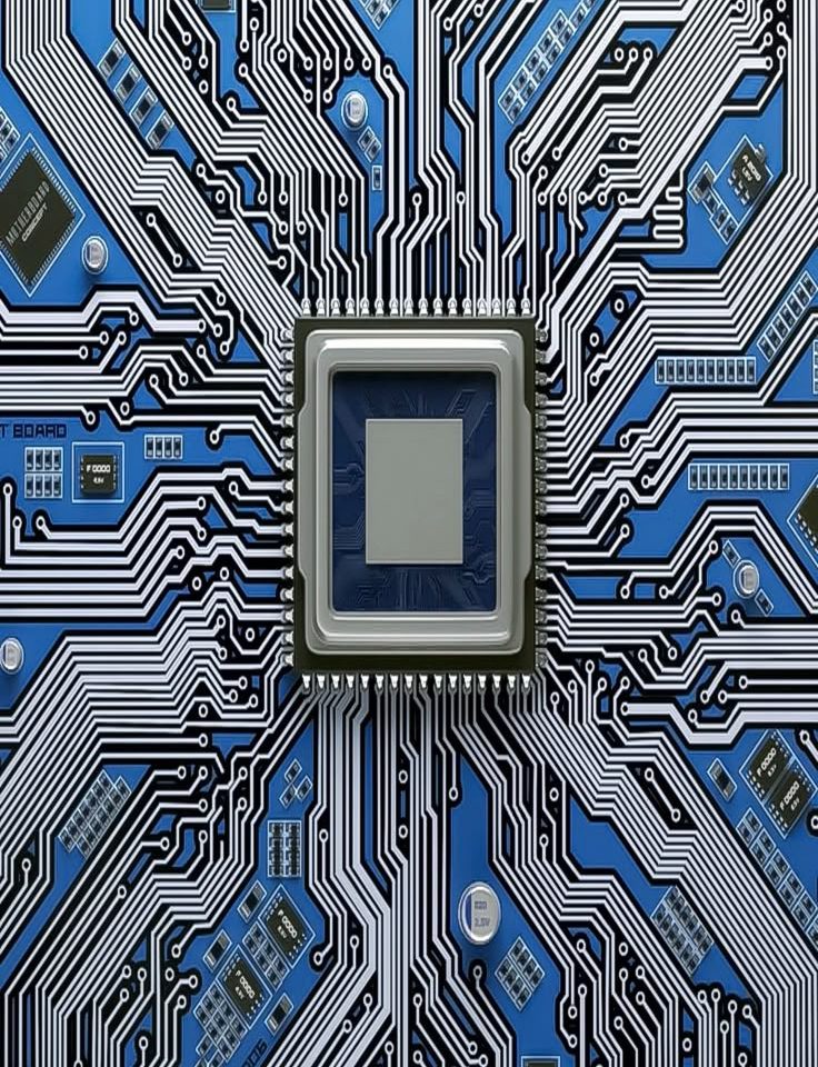 Routing & Switching Silicon for AI NetworksRouting and switching silicon for service-provider, web-scale and AI networksExplore more
 Coherent DSP & Optical Interconnect IntegrationCoherent DSPs and fiber-optic chips: the links that carry AI trafficExplore more



PrimeSilicon's team caught issues weeks before they became costly. Their communication throughout the tapeout was exceptional.
PrimeSilicon's PNR methodology is rock solid. Clean floorplans, tight timing closure, and clear documentation every step of the way.

Reach out to our Cupertino headquarters — 10080 N. Wolfe Rd., Suite SW3-282, Cupertino, CA 95014, United States. Our team is ready to discuss your next tapeout.
info@primesilicon.com
PrimeSilicon Technology Inc.
10080 N. Wolfe Rd.
Suite SW3-282 , Cupertino , CA 95014 , United States
PrimeSilicon Technology (BD) Ltd. ENA Tower (Level-4), Plot 57/3, West Panthapath, Dhaka-1205, Bangladesh